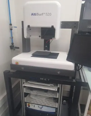
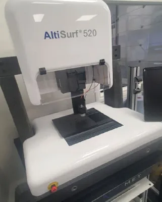
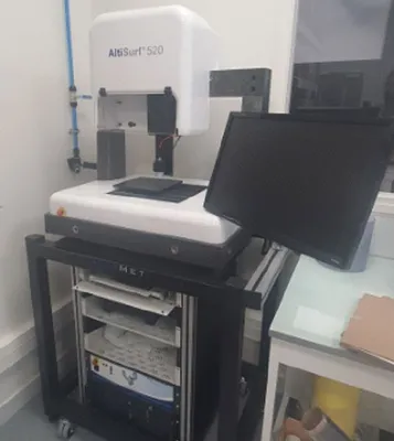
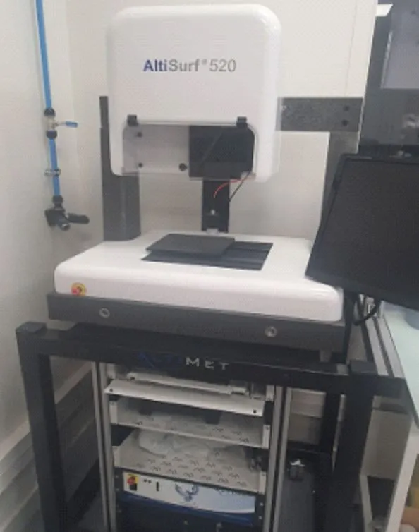
<p>Make: Altimet<br>Model: Altisurf 520<br>Serial No: 0815-A520-03/165<br>Year of Commissioning: 2023<br>Condition: LIKE NEW, Limited R&D Usage by a doctoral student, maintained in lab environment<br>Can Be Demonstrated on site or remote session - Complete technical datasheets, test reports, and software tutorials are available on request.</p>
<p>Includes Altimap Software for date analysis and 3D rendering</p>
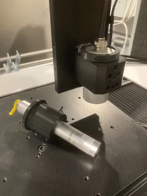
<p>2D and 3D Surface Characterization, Topography, Roughness, Flatness, Step Height<br>Non Contact Optical Profilometer using chromatic con focal and or interferometric sensors</p>
<figure><img src="https://machinerymanager.com/rails/active_storage/blobs/redirect/eyJfcmFpbHMiOnsiZGF0YSI6NjI4NzY1NjIsInB1ciI6ImJsb2JfaWQifX0=--dc41c10c9222296aa5b28c6f627443c9f15bd602/image.png"></figure><p><br><br></p>
<p><b>Features And Benefits: </b></p>
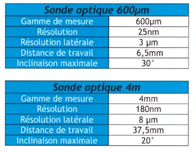
<p>⦁ Measurement range (Z-axis): up to 350 µm<br>⦁ Resolution: Nanometer precision (down to 5 nm depending on sensor)<br>⦁ Scanning speed: Up to 300,000 points per second<br>⦁ Surface parameters: Ra, Rz, Rq, Sa, Sz, Sq, step height, waviness, flatness, form<br>⦁ Sensor compatibility: Chromatic confocal, interferometric, or hybrid (depending on configuration)<br>⦁ XY stage: Motorized, programmable for scanning of large parts<br>⦁ User software: Altimap – for intuitive control, real-time 3D visualization and data export</p>
<p></p>
<p><b>Typical Applications: </b></p>
<p>⦁ Micro-roughness analysis on metals, polymers, and ceramics<br>⦁ Topographical mapping of structured or coated surfaces<br>⦁ Step height and layer thickness measurement in MEMS and microelectronics<br>⦁ Quality control in surface finishing and material science<br>⦁ Research and development in thin films, printed electronics, and biomedical surfaces</p>
<p></p>
<p><b>Ideal For: </b></p>
<p>⦁ R&D laboratories<br>⦁ Surface engineering and material science teams<br>⦁ Precision manufacturing quality control<br>⦁ Printed electronics and thin film research<br>⦁ Biomedical device prototyping</p>
<ul></ul>